Page 99 - Physics - XII
P. 99
Circuit Diagram to Draw Reverse Bias Characteristic
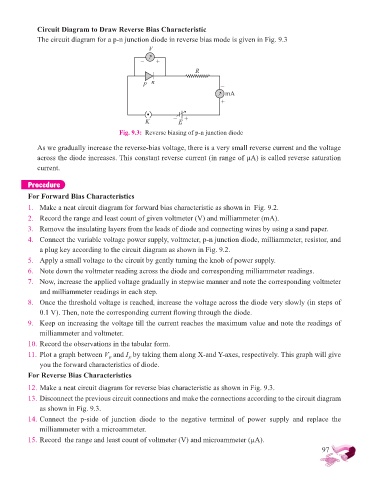
                The circuit diagram for a p-n junction diode in reverse bias mode is given in Fig. 9.3
                                                   V

                                                 –    +
                                                                   R
                                                  p  n                      –

                                                                             mA
                                                                            +


                                                  K         –  E  +
                                         Fig. 9.3:  Reverse biasing of p-n junction diode

                As we gradually increase the reverse-bias voltage, there is a very small reverse current and the voltage
              across the diode increases. This constant reverse current (in range of µA) is called reverse saturation
              current.


          Procedure
          For Forward Bias Characteristics

          1.  Make a neat circuit diagram for forward bias characteristic as shown in  Fig. 9.2.
          2.  Record the range and least count of given voltmeter (V) and milliammeter (mA).
          3.  Remove the insulating layers from the leads of diode and connecting wires by using a sand paper.
          4.  Connect the variable voltage power supply, voltmeter, p-n junction diode, milliammeter, resistor, and

              a plug key according to the circuit diagram as shown in Fig. 9.2.
          5.  Apply a small voltage to the circuit by gently turning the knob of power supply.
          6.  Note down the voltmeter reading across the diode and corresponding milliammeter readings.
          7.  Now, increase the applied voltage gradually in stepwise manner and note the corresponding voltmeter
              and milliammeter readings in each step.

          8.  Once the threshold voltage is reached, increase the voltage across the diode very slowly (in steps of
              0.1 V). Then, note the corresponding current fl owing through the diode.
          9.  Keep on increasing the voltage till the current reaches the maximum value and note the readings of
              milliammeter and voltmeter.
          10. Record the observations in the tabular form.

          11. Plot a graph between V  and I  by taking them along X-and Y-axes, respectively. This graph will give
                                            F
                                      F
              you the forward characteristics of diode.
          For Reverse Bias Characteristics

          12. Make a neat circuit diagram for reverse bias characteristic as shown in Fig. 9.3.
          13. Disconnect the previous circuit connections and make the connections according to the circuit diagram
              as shown in Fig. 9.3.
          14. Connect  the  p-side  of  junction  diode  to  the  negative  terminal  of  power  supply  and  replace  the
              milliammeter with a microammeter.

          15. Record  the range and least count of voltmeter (V) and microammeter (µA).
                                                                                                              97

