Page 98 - Physics - XII
P. 98
Semiconductor Electronics:
                                          Semiconductor Electronics:
                 5                        Materials, Devices and
                                          Materials, Devices and
                                          Simple Circuits
                                          Simple Circuits


                                                       EXPERIMENT - 9


              Aim
              To draw the I-V characteristic curve for a p-n junction diode in forward and reverse bias.

              Apparatus and Materials Required

              A p-n junction diode (or semiconductor diode), a resistor of value 3 Ω, a variable voltage power supply
              (0–12 V), a voltmeter (0–12 V), a milliammeter (0–200 mA), a microammeter (0–200 µA), a one-way
              key, connecting wires, and a piece of sand paper


              Principle/Theory
              A p-n junction diode consists of wafers of p-type and n-type semiconductors fused together or grown
              on each other.


                                                              p     n
                                                Fig. 9.1:  Symbol of p-n junction diode


              Forward and Reverse Biasing of Diode
              When an external voltage is applied to a p-n junction, then two types of biasing may take place.
                (i)   A diode is said to be forward biased, if its p-side is connected to the positive terminal of the battery
                   and n-side to the negative terminal of the battery.
               (ii)   A diode is said to be reverse biased, if its p-side is connected to the negative terminal of the battery
                   and n-side to the positive terminal of the battery.
                                                                                           V
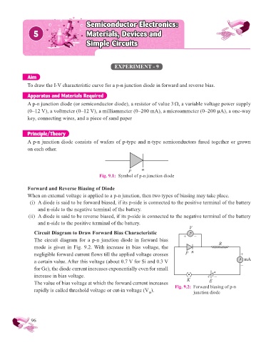
                 Circuit Diagram to Draw Forward Bias Characteristic
                   The  circuit  diagram  for  a  p-n  junction  diode  in  forward  bias   +  –
                 mode  is  given  in  Fig.  9.2. With  increase in  bias  voltage, the                   R
                 negligible forward current fl ows till the applied voltage crosses       p n                       +
                 a certain value. After this voltage (about 0.7 V for Si and 0.3 V                                   mA
                 for Ge), the diode current increases exponentially even for small                                 –
                 increase in bias voltage.                                                         + –

                   The value of bias voltage at which the forward current increases       K         E
                 rapidly is called threshold voltage or cut-in voltage (V ).        Fig. 9.2:  Forward biasing of p-n
                                                                       th                    junction diode


                96

