Page 105 - Physics - XII
P. 105
Q9.  A diode’s reverse current is of the order of
                  (a)  kA                  (b)  mA                  (c)  µA                   (d)  A

           Q10.  What will happen when a p-n diode is reversed-biased?
                  (a)  No current fl ows.                            (b) The depletion region is increased.

                  (c)  The depletion region is reduced.             (d) The height of the potential barrier is reduced.

           Answer key

               1. (c), 2. (b), 3. (a), 4. (a), 5. (b),  6. (a), 7. (b), 8. (c), 9. (c), 10. (b)


          Case Study-based Questions

          Read the paragraph and answer the questions that follow.
          The process of applying the external voltage to a p-n junction semiconductor diode is called biasing.
          When the positive terminal of the source is connected to the p-side and the negative terminal is connected

          to n-side, then the junction diode is said to be connected in forward bias condition. When this external
          voltage exceeds the threshold voltage, the current starts increasing exponentially. The value of threshold
          voltage for silicon diode is 0.7 V and for germanium diode is 0.3 V.

          When the positive terminal of the source is connected to the n-side and the negative terminal is connected
          to  p-side,  then  the  junction  diode  is  said  to  be  connected  in  reverse  bias  condition.  In  reverse  bias
          conditions, a very small reverse current fl ows through the diode which is called reverse saturation current.

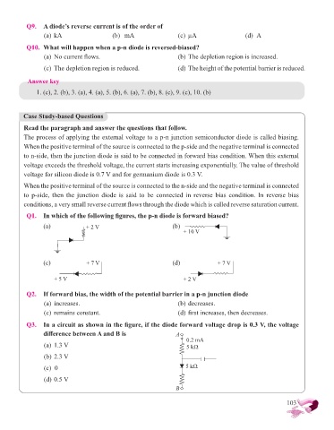
           Q1.   In which of the following fi gures, the p-n diode is forward biased?
                 (a)             + 2 V                            (b)
                                                                      + 10 V


                 (c)              + 7 V                           (d)              + 7 V


                     + 5 V                                            + 2 V

           Q2.  If forward bias, the width of the potential barrier in a p-n junction diode
                  (a)  increases.                                   (b) decreases.
                  (c)  remains constant.                            (d) fi rst increases, then decreases.

           Q3.  In a circuit as shown in the fi gure, if the diode forward voltage drop is 0.3 V, the voltage
                 diff erence between A and B is                     A
                                                                       0.2 mA
                  (a)  1.3 V                                           5 kΩ

                  (b) 2.3 V

                  (c)  0                                               5 kΩ
                  (d) 0.5 V
                                                                   B


                                                                                                             103

